Were it not for the thin sheath of water and carbon-based life covering it, our home planet would perhaps be best known as the “Silicon World.” More than a quarter of the mass of the Earth’s crust is silicon, and together with oxygen, the silicate minerals form about 90% of the thin shell of rock that floats on the Earth’s mantle. Silicon is the bedrock of our world, and it’s literally as common as dirt.
But just because we have a lot of it doesn’t mean we have much of it in its pure form. And it’s only in its purest form that silicon becomes the stuff that brought our world into the Information Age. Elemental silicon is very rare, though, and so getting appreciable amounts of the metalloid that’s pure enough to be useful requires some pretty energy- and resource-intensive mining and refining operations. These operations use some pretty interesting chemistry and a few neat tricks, and when scaled up to industrial levels, they pose unique challenges that require some pretty clever engineering to deal with.
Hard as Rock
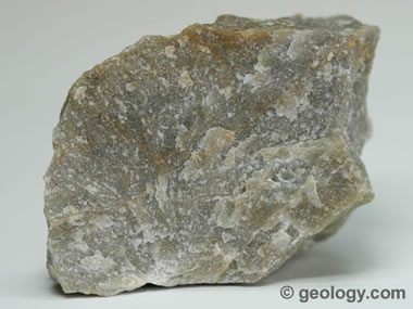
The raw material for most silicon production is the mineral quartzite. Quartzite comes from ancient deposits of quartz sands that formed sedimentary deposits. Over time and with heat and pressure, these quartz sandstones were transformed into the metamorphic rock quartzite, which is at least 80% quartz by volume.

Quartzite is an incredibly tough rock, and where it pokes above the surface, it forms ridges that strongly resist weathering. Significant formations of quartzite are scattered all around the world, but there are relatively few places where it makes financial sense to quarry the rock for silicon production, since the formations need to be easily accessible and relatively close to the other raw materials and energy supply needed.
Raw quartzite is mostly silicon dioxide (SiO2), and the refining process begins with a reduction reaction to get rid of the oxygen. Crushed quartzite is mixed with carbon in the form of coke (coal that has been heated in the absence of oxygen). Woodchips are added to the charge as well; they serve both as a carbon source and a physical bulking agent that allows gasses and heat to circulate better in the furnace.
The arc furnaces for silicon smelting are massive installations with huge carbon electrodes. The electrodes are consumed during smelting, so new electrodes are screwed onto the tops of the current electrodes to make sure the process isn’t interrupted. The arc furnace requires massive amounts of electricity to maintain the 2,000°C temperature needed, so silicon refineries are often located where electricity is cheap and plentiful.
The reduction reactions inside the melt zone are actually pretty complicated, but can be summed up with two main reactions:
In both reactions, the oxygen in the silicon dioxide combines with carbon to form the main waste product, carbon monoxide. A side reaction that occurs in a part of the melt zone inside the furnace produces silicon carbide (SiC), which is an unwanted byproduct (at least when the goal is to purify silicon; silicon carbide itself is a useful industrial abrasive). By making sure that silicon dioxide is far in excess in the furnace, the second reaction where the SiC acts as a carbon source for the reduction of silicon dioxide is favored, and silicon with up to 99% purity can be tapped off the bottom of the furnace.
The silicon produced by this process is referred to as metallurgical silicon. For almost all industrial uses, this highly purified silicon is good enough. About 70% of metallurgical silicon goes to the manufacture of metal alloys such as ferrosilicon as well as aluminum-silicon, an alloy that contracts minimally upon cooling and is therefore used to cast aluminum engine blocks and similar items.
More Nines

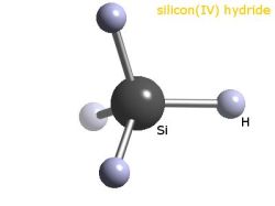
As useful as metallurgical silicon is, even at 99% pure it’s not even close to the purity needed for semiconductor and photovoltaic applications. The next steps in purification take the silicon to the purity level that’s needed for semiconductor manufacture. Purification starts by mixing powdered metallurgical silicon with hot, gaseous hydrochloric acid. This reaction produces silanes, which are compounds with a central silicon atom surrounded by four attachments, in this case three chlorine atoms and one hydrogen. This trichlorosilane is a gas at the temperature inside the reaction chamber, which makes it easier to handle and purify by fractional distillation.
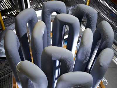
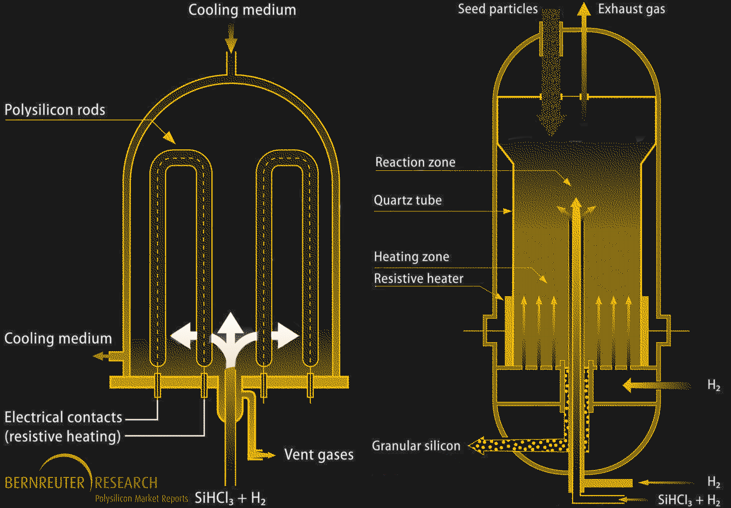
When the trichlorosilane gas has been sufficiently purified, polycrystalline silicon production can begin. The Siemens process is the main method here, and is a form of chemical vapor deposition. A large bell-shaped reaction chamber contains several thin threads of highly purified silicon, which are heated to 1,150°C by passing an electric current through them. A mixture of gaseous trichlorosilane and hydrogen flows into the chamber; the gas decomposes on the hot electrode leaving behind the silicon, which accretes into rods that are about 15 cm in diameter. Polycrystalline silicon made by the Siemens process can have a purity of 99.99999% (“seven nines”, or 7N) or more. 7N to 10N polysilicon is mostly used for photovoltaic cells, although some polysilicon in this purity range also makes it into MOSFET and CMOS semiconductors.

While the Siemens process is the polysilicon workhorse, it has its disadvantages. The main problem is that it’s an energy hog — keeping the growing polycrystalline rods hot enough to decompose the feedstock requires a lot of electricity. To work around this problem, a fluidized bed reactor (FBR) process is sometimes used. An FBR reactor is shaped like a tall tower, the walls of which are lined with a quartz tube. Silane gas, either the familiar trichlorosilane or monosilane, which is just a silicon atom surrounded by four hydrogens, is injected into the chamber. Powdered silicon is dropped into the reaction chamber from the top, while heated hydrogen gas is injected into the bottom of the chamber through a series of nozzles. The gas flow keeps the hot silicon powder fluidized, allowing it to mix with the silane gas and decompose it. As in the Siemens process, the silicon accretes onto the seed particles, which eventually get too large for the fluidized bed to support. The polycrystalline silicon beads drop to the bottom of the chamber, where they can be collected.
Aside from power savings — up to 90% less when using monosilane as a feedstock — the FBR method’s main advantage is that it’s a continuous process, since the finished beads can just be pumped out of the chamber. The Siemens process is more of a batch process, since the reactor chamber has to be opened to remove the polysilicon rods when they’re finished. That said, FBR polysilicon hasn’t really taken off, in part because managing the fluid dynamics inside the reaction chamber can be difficult. But the main reason is that the Siemens process is just so easy, and as long as factories can be located near a source of cheap electricity, it’s just easier to use the brute-force method.

One Crystal Only, Please
Using either of these methods, polycrystalline silicon can be brought to extremely high purity, up to 11N. But purity isn’t the only metric for silicon; sometimes, the nature of the crystalline structure on the end product is just as important as purity. The next step in silicon production is the creation of monocrystalline silicon, where the entire silicon ingot is a single crystal.
Growing a single crystal of ultra-pure silicon to a size that’s industrially useful is no mean feat, and relies on some tricks discovered in 1916 by Polish chemist Jan Czochralski. We’ve covered the Czochralski method in depth before, but briefly, polycrystalline silicon is melted in a quartz crucible in an inert atmosphere. A puller rod bearing a single ultra-pure silicon crystal that is very precisely oriented is lowered into the molten silicon. The seed crystal causes silicon to condense, continuing the crystal structure as the puller rod is slowly withdrawn from the furnace while rotating. Single-crystal ingots up to 450 mm in diameter are possible with the Czochralski method.
Another method to produce monocrystalline silicon is the float zone method, which uses a polycrystalline silicon rod as the starting material. Inside a reaction chamber with an inert gas atmosphere, a radio frequency signal is passed through a coil that surrounds the rod. The RF signal heats the polysilicon, creating a confined melt zone. Single crystals of ultra-pure silicon are added to the melt zone, which causes the molten silicon to crystallize around it. The RF coil is slowly moved up the rod, moving the zone of heating until the entire rod is a single crystal of silicon. Float-zone monocrystalline silicon has the advantage of never being in contact with the quartz walls of the Czochralski method crucible, and so will have less contamination from oxygen and other impurities.
No comments:
Post a Comment